
FAQ - Frequently Asked Questions
Here are some of the most frequently asked questions regarding our products and services.
Files for conductor layers, solder masks, component silkscreen, board outline, drilling diagram, mechanical drawings (panelization), carbon paste, cradle, solder-out (peelable), and solder paste—all in Gerber RS274-X format. The drilling file should be in NC-Drill ASCII format, the technical specifications in Document format, and the CAD NetList in IPC-D-356 or IPC-D-356A format, or alternatively, the files exported in ODB++ format, for layout integrity verification.
Each CAD tool has its own export process, but in most cases, the files can be accessed through the Data Export menu (Gerber, CAM, etc.).
There is some visualization software available for download on the internet, the most common of which are listed below:
www.pentalogix.com
www.gerber-viewer.com
www.circuitpeople.com
gerbv.gpleda.org for the Linux platform.
-Plate thickness, measurement location, tolerance and base copper thickness;
-Drilling tolerance;
– Copper deposition inside plated holes;
– Board outline tolerance;
-Solder mask color;
-Symbology color;
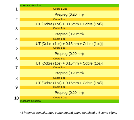
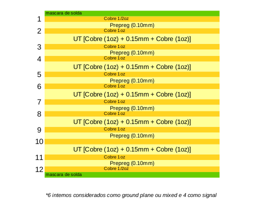
-Stackup (for multilayer boards);
– V-cut core and its tolerance (for boards with V-scoring finish);
– Drilling diagram indicating the diameters of plated and non-plated holes, as well as all cutouts (slots) present on the board;
-If it is necessary to manufacture the panel, the desired layout, number of panels and whether false edges should be added (an illustrative drawing may be used);
All relevant PCB mechanical dimensions for the customer must be documented in a mechanical drawing provided along with the Gerber files.
It is worth noting that any additional finishes such as peelable solder mask, via plugging, or carbon ink must be clearly specified.
Board Thickness: 1.60 mm ±0.19 mm – Solder Mask Color: Green – Silkscreen Color: White – Minimum Solder Mask Thickness: 8 µm – Surface Finish: HAL – Hot Air Leveling – (Sn 63%, Pb 37%) – Drilling: Plated holes up to 6.40 mm and non-plated holes up to 6.50 mm ±0.10 mm. Plated holes larger than 6.40 mm and non-plated holes larger than 6.50 mm ±0.20 mm – Mechanical Tolerance: ±0.20 mm – V-cut Tolerance: Core of 0.40 mm ±0.10 mm – Tg: 150°C – Td: 310°C
IPC A 600 (Class 2)
Gerber file containing the panelization features and other adjustments that will be applied to the boards, provided for customer review and approval.
It is obtained from the following formula:
Minimum ring = Di - Db / 2, where:
(Di: diameter of the island corresponding to the hole in question;
Db: diameter of the drill bit* to be used for drilling.
Drill bit*: The drill bit is the tool used in a CNC machine to drill the PCB. The diameter of this drill bit will be determined by the PCB manufacturer taking into account the drilling tolerance).
Example: A given metallized hole has a final diameter of 0.50mm. Its drilling tolerance is +/-0.10mm. The drill bit used to drill the PCB will be 0.60mm, because copper will still be added to this hole, so that at the end of this stage it will return to the original final diameter of 0.50mm. We recommend a minimum ring size of at least 0.12mm (5mil).
They are isolated pads on the internal layers. These pads are not required for metallization and can be safely removed either through CAD software settings or by the CAM software during data preparation.
Drill*: The drill bit is the tool used in a CNC machine to drill the PCB. The diameter of this drill bit will be determined by the PCB manufacturer taking into account the drilling tolerance).
Example: A given metallized hole has a final diameter of 0.50mm. Its drilling tolerance is +/-0.10mm. The drill bit used to drill the PCB will be 0.60mm, because copper will still be added to this hole, so that at the end of this stage it will return to the original final diameter of 0.50mm. We recommend a minimum ring size of at least 0.12mm (5mil).
Yes. For routed edges: 0.30 mm (12 mils) for external layers and 0.50 mm (20 mils) for internal layers. For V-scored edges: 0.35 mm (14 mils) for external layers and 0.50 mm (20 mils) for internal layers.
Yes. The inclusion of inscriptions assists in identifying the board (code and revision) and the layers (assembly sequence).
Yes. This identification shows the holes that should be unmetallized after the plate is finished.
HAL - Hot Air Leveling - Sn 63% + Pb 37%. Does not comply with the RoHS directive; OSP - Organic Solderability Preservative - Copper Passivation. Meets the RoHS directive and ENIG - Electroless Nickel Immersion Gold. Meets the RoHS directive.
This is the reference that will be used to align the boards for component assembly and/or functional tests.
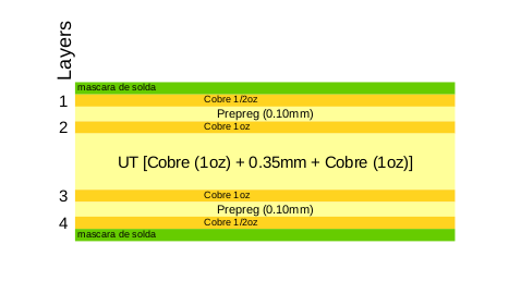
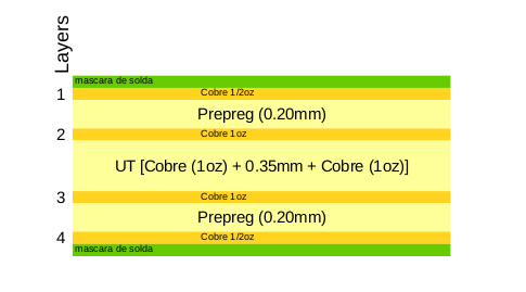
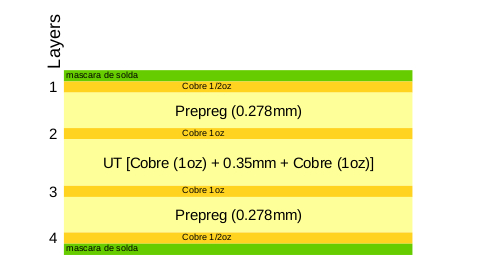
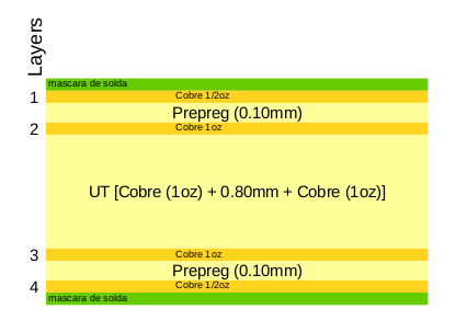
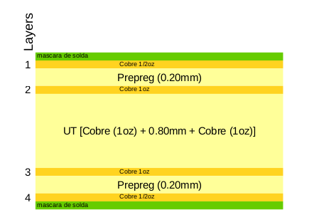
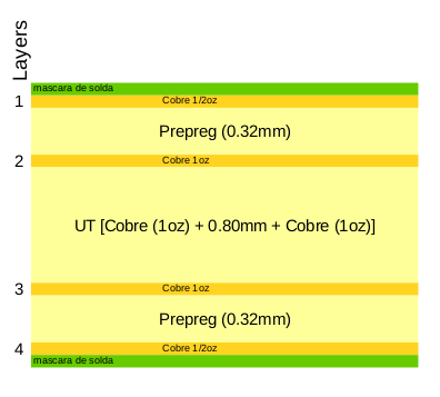
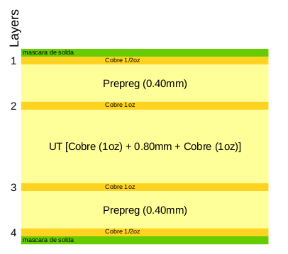
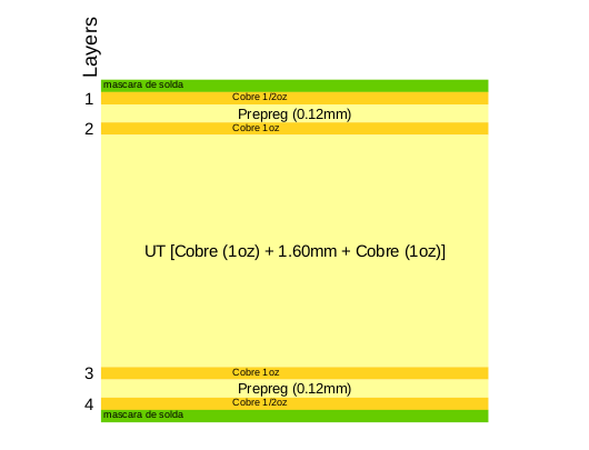
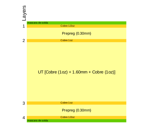
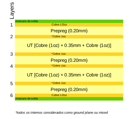
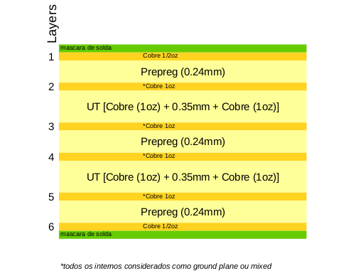
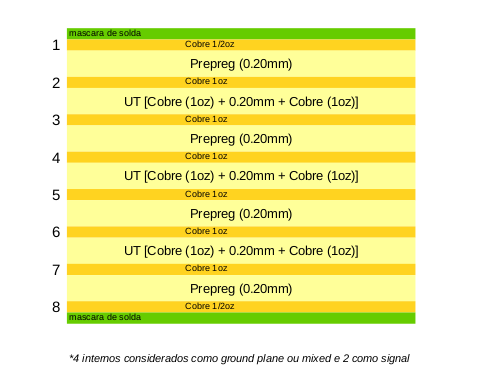
This is a representation of the construction of the insulating and conductive substrate(s) of a printed circuit board, as well as the sequential order of the conductive layers. Copper passivation. Complies with the RoHS directive and ENIG - Electroless Nickel Immersion Gold. Complies with the RoHS directive.
Thickness: 0.80m
Thickness measurement location: total (copper platting + solder mask)
Stackup (click here)
Thickness: 1.00m
Thickness measurement location: total (copper platting + solder mask)
Stackup
Thickness measurement location: base laminate
Stackup
Thickness: 1.20m
Thickness measurement location: total (copper platting + solder mask)
Stackup
Thickness measurement location: base laminate
Stackup
Thickness: 1.60m
Thickness measurement location: total (copper platting + solder mask)
Stackup
Thickness measurement location: base laminate
Stackup
Thickness: 2.00m
Thickness measurement location: total (copper platting + solder mask)
Stackup
Thickness: 2.40m
Thickness measurement location: total (copper platting + solder mask)
Stackup
Thickness: 1.60m
Thickness measurement location: total (copper platting + solder mask)
Stackup (click here)
Thickness measurement location: base laminate
Stackup
Thickness: 1.60m
Thickness measurement location: base laminate
Stackup (click here)
Thickness: 1.60m
Thickness measurement location: base laminate
Stackup (click here)
Thickness measurement location: base laminate
Stackup
Thickness: 1.60m
Thickness measurement location: base laminate
Stackup (click here)